Dislocations and structure of nitrides
The main problem that constricts nitride-based future developments is the variable structural quality of nitride thin films because of the lattice mismatch between them and the substrates used to grow this material. Dislocation densities in GaN films can range from 108 to 1010 dislocations per square centimetre [1].
Dislocations reduce the efficiency of diodes as they act as nonradiative recombination centres. They also degrade the conductivity of the material which restricts efficiency and power of nitrides in electrical devices.
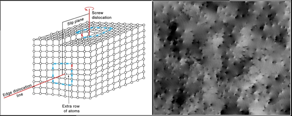
left: schematic of lattice dislocation | right: ECC image of GaN thin film
We investigate methods to reveal dislocations in nitride thin films. We map tilt, twist and strain and study their relationship to the distribution and densities of defects. Future work includes identifying the role of defects in the performance of nitride based devices on a nanometre scale and simulating dislocation contrast via dynamical electron scattering calculations.
Tuning nitrides – alloys and rare earth doping
We study the emission properties of nitride ternary alloys and their potential applications.
With GaN being ahead in the race of nitrides towards new applications, alloys allow a greater tunability, e.g. the ternary alloy InxGa1-xN emits light from violet to amber, dependent on the relative fraction of In. While changing the alloys composition offers different features, it also affects efficiency and quality of the doped material.
Another approach to tune properties of III-nitrides is the implantation of rare earth ions. These ions act as a luminescence centre, radiating at a different wavelength. The emission of the nitride host and rare earth implant mixes and results in new LED colors. Our team is currently dealing with lattice location and cathodoluminescence of rare earth doped alloys.
Characterisation methods
We are presently using attractive characterisation methods to probe the structural and luminescence properties of III-nitrides on the nanoscale:
- Wavelength-dispersive X-ray (WDX) spectroscopy
WDX uses a fixed-wavelength x-ray diffracted by the material under study and provides a quantitative measure of its composition. - Cathodoluminescence (CL) hyperspectral imaging
CL detects the luminescence spectrum of the sample which is sensitive to strain, crystallinity, defects, doping and free carrier concentration. Cathodoluminescence gives information about composition, growth and quality of the material with resolutions up to 10-20nm. We have developed a system for simultaneusly acquiring hyperspectral CL together with high-sensitivity WDX maps to correlate composition and luminescence properties [2]. For example InN fluctuations in InxGa1-xN thin films have been measured on a scale of tens of nanometres [3]. - Electron backscatter diffraction (EBSD)
EBSD, also known as ”backscatter Kikuchi diffraction”, uses electron backscattering on highly tilted samples to produce a 2-D projection of the crystal structure. We deduced that EBSD patterns acquired from a mesh of points on a sample can be used to produce maps of crystal structure with a resolution of ca. 20nm, measure orientation schanges of the order of 0.02° and strain changes of 2×10⁻⁴ in III-nitride thin films [4]. - Electron channeling contrast imaging (ECCI)
ECCI derives images of electrons channeling down the crystal planes of a tilted sample. These images reveal defects which distort the crystal planes with a resolution of tens of nanometres. We deduced that ECCI is suitable for imaging tilt, atomic steps and threading dislocations in III-nitride thin films. - Extended X-Ray absorption fine structure (EXAFS)
EXAFS allows the acquisition of information about the local environment of a specific elemental species by analysing oscillations in X-ray absorption versus photon energy. These oscillations are caused by interference of backscattered electrons with the original X-rays.
EXAFS provides complementary information to that provided by the microscopy techniques listed above, for example, the chemical bonding, coordination numbers and bond lengths. Statistical information about the first few moments of the spatial distribution of near neighbours around a targeted atomic species can be obtained (e.g. Ga in an InGaN thin film).
[1] H. Marchand, X. H. Wu, J. P. Ibbetson, P. T. Fini, P. Kozodoy, S. Keller, J. S. Speck, S. P. DenBaars, and U. K. Mishra, “Microstructure of GaN laterally overgrown by metalorganic chemical vapor deposition,” Applied Physics Letters, vol. 73, iss. 6, pp. 747-749, 1998.
[2] R. W. Martin, P. R. Edwards, K. P. O’Donnell, M. D. Dawson, C. W. Jeon, C. Liu, G. R. Rice, and I. M. Watson, “Cathodoluminescence spectral mapping of III-nitride structures,” Physica Status Solidi A, vol. 201, iss. 4, pp. 665-672, 2004.
[3] P. R. Edwards, R. W. Martin, K. P. O’Donnell, and I. M. Watson, “Simultaneous composition mapping and hyperspectral cathodoluminescence imaging of InGaN epilayers,” Physica Status Solidi C, iss. 7, pp. 2474-2477, 2003.
[4] C. Trager-Cowan, F. Sweeney, A. Winkelmann, A. J. Wilkinson, P. W. Trimby, A. P. Day, A. Gholinia, N. H. Schmidt, P. J. Parbrook, and I. M. Watson, “Characterisation of nitride thin films by electron backscatter diffraction and electron channelling contrast imaging,” Materials Science and Technology, vol. 22, iss. 11, pp. 1352-1358, 2006.
Fred Schubert, “Light-emitting diodes hit the centenary milestone”, Compound Semiconductor, Oct 15, 2007.